跳转到主要内容

二维材料实验室

晶圆级二维材料制备与器件研究

简介
  课题组围绕二维材料及其范德华异质结构的可控制备、物理机制与器件应用开展研究。 重点发展晶圆级、高结晶质量二维材料的化学气相沉积生长方法, 并探索其在新型电子与光电子器件中的应用潜力。

  研究工作面向基础科学问题与未来信息器件需求, 致力于推动二维材料从实验室研究向规模化集成应用转化发展。

课题组简介

二维材料与范德华异质结构实验室致力于二维材料体系的高质量生长、结构调控与片上集成研究。 围绕石墨烯、六方氮化硼(h-BN)及过渡金属硫族化合物(TMDs)等代表性二维材料, 系统开展从生长机理、结构表征到器件物理的多尺度研究。

课题组重点关注材料生长过程中结晶质量、取向一致性及界面结构 对材料物性与器件性能的影响, 探索兼顾基础研究深度与器件应用潜力的二维材料研究路径。
研究方向

研究方向

  • 晶圆级二维材料的可控制备
    发展面向晶圆尺度的二维材料化学气相沉积(CVD / CVT)生长方法, 探索无核化、高结晶质量、取向一致的单晶二维材料制备机制, 为大面积器件集成奠定材料基础。

  • 二维材料的无转移生长与片上集成
    探索超低温、无转移生长策略, 实现二维材料在绝缘衬底及功能基底上的直接生长, 降低界面污染与结构损伤, 提升器件一致性与可靠性。

  • 范德华异质结构的物性与器件应用
    构筑高质量二维范德华异质结, 系统研究其电学、光学及界面物理特性, 探索其在新型电子器件、光电器件及忆阻器等方向的应用潜力。

代表性研究成果

Wafer-scale single-crystal monolayer graphene grown on sapphire substrate

The growth of inch-scale high-quality graphene on insulating substrates is desirable for electronic and optoelectronic applications, but remains challenging due to the lack of metal catalysis. Here we demonstrate the wafer-scale synthesis of adlayer-free ultra-flat single-crystal monolayer graphene on sapphire substrates. We converted polycrystalline Cu foil placed on Al2O3(0001) into single-crystal Cu(111) film via annealing, and then achieved epitaxial growth of graphene at the interface between Cu(111) and Al2O3(0001) by multi-cycle plasma etching-assisted–chemical vapour deposition. Immersion in liquid nitrogen followed by rapid heating causes the Cu(111) film to bulge and peel off easily, while the graphene film remains on the sapphire substrate without degradation. Field-effect transistors fabricated on as-grown graphene exhibited good electronic transport properties with high carrier mobilities. This work breaks a bottleneck of synthesizing wafer-scale single-crystal monolayer graphene on insulating substrates and could contribute to next-generation graphene-based nanodevices.

Paper

Single-crystal hBN monolayers from aligned hexagonal islands

Hexagonal boron nitride (hBN), as one of the few two-dimensional insulators, holds strategic importance for advancing post-silicon electronic devices and circuits. Achieving wafer-scale, high-quality monolayer hBN is essential for its integration into the semiconductor industry. However, the physical mechanisms behind the chemical vapor deposition (CVD) synthesis of hBN are not yet well understood. Investigating morphology engineering is critical for developing scalable synthetic techniques for the large-scale production of high-quality hBN. In this study, we explored the underlying mechanisms of the CVD growth process of hBN and found that the involvement of a small amount of oxygen effectively modulates the shape of the single-crystal hBN islands. By tuning the oxygen content in the CVD system, we synthesized well-aligned hexagonal hBN islands and achieved a continuous, high-quality single-crystal monolayer hBN film through the merging of these hexagonal islands on conventional single-crystal metal-foil substrates. Density functional theory was used to study the edges of hBN monolayers grown in an oxygen-assisted environment, providing insights into the formation mechanism. This study opens new pathways for controlling the island shape of 2D materials and establishes a foundation for the industrial-scale production of high-quality, large-area, single-crystal hBN.

Paper

Nonepitaxial wafer‐scale single‐crystal 2D materials on insulators

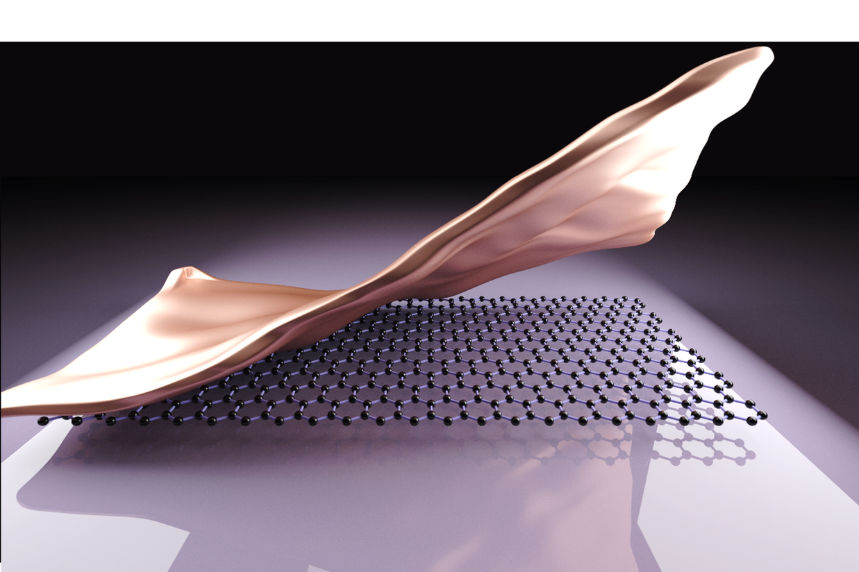
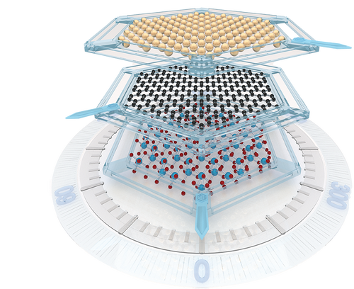
Next-generation nanodevices require 2D material synthesis on insulating substrates. However, growing high-quality 2D-layered materials, such as hexagonal boron nitride (hBN) and graphene, on insulators is challenging owing to the lack of suitable metal catalysts, imperfect lattice matching with substrates, and other factors. Therefore, developing a generally applicable approach for realizing high-quality 2D layers on insulators remains crucial, despite numerous strategies being explored. Herein, a universal strategy is introduced for the nonepitaxial synthesis of wafer-scale single-crystal 2D materials on arbitrary insulating substrates. The metal foil in a nonadhered metal–insulator substrate system is almost melted by a brief high-temperature treatment, thereby pressing the as-grown 2D layers to well attach onto the insulators. High-quality, large-area, single-crystal, monolayer hBN and graphene films are synthesized on various insulating substrates. This strategy provides new pathways for synthesizing various 2D materials on arbitrary insulators and offers a universal epitaxial platform for future single-crystal film production.

Paper

学术交流与合作

低维磁性材料专家


学术交流与合作

Prof. Xixiang Zhang

KAUST, Saudi Arabia

二维半导体材料专家


学术交流与合作

Prof. Zheng liu

NTU, Singapore

石墨烯碳材料专家


学术交流与合作

Prof. Rodney Ruoff

UNIST, South Korea

加入我们

课题组欢迎对二维材料制备及器件应用研究感兴趣的本科生、硕士生和博士生加入团队,长期招收二维材料相关方向博士后研究人员。请通过电子邮件与我联系。

同时,也欢迎与国内外相关领域研究团队开展学术交流与合作。 有意者请通过邮件联系,简要介绍研究背景与兴趣方向。

研究理念

探索底层物理机制

制备晶圆级二维材料

面向未来高集成芯片器件